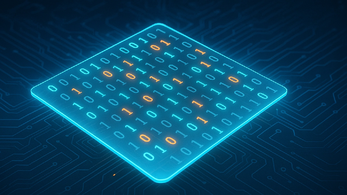
Swedish scientists at Chalmers University of Technology have engineered an atom-thin magnetic material that could cut the power consumption of memory chips by up to 90 %. This could be a turning point for energy-efficient electronics, where every watt saved matters.
At its core, the innovation combines two opposing magnetic orders in a single ultra-thin layer, enabling memory states to flip with much less energy. If scaled, this could transform how devices from smartphones to data centers store information.
How the Atom-Thin Material Works
To understand the novelty, imagine a seesaw whose balance point can be nudged with a light tap rather than a full push. Traditional magnetic memory uses stacked layers and external magnetic fields — energy-intensive — to flip states.
The material developed, called (Co₀.₅Fe₀.₅)₅₋ₓGeTe₂ (“CFGT”), hosts both ferromagnetic and antiferromagnetic orders in the same atomic layer. This “tilted magnetism” allows switching of memory bits with much lower energy input.
This discovery was reported by ScienceBlog: “Swedish researchers have developed an atomically thin material that could dramatically slash the energy consumption of computer memory chips.” ScienceBlog article on the breakthrough
In contrast to conventional designs, the new material does away with multiple interfaces and redundant layers, simplifying fabrication.
Why This Matters: Energy, Heat & Device Efficiency
Modern memory chips already demand high energy, contributing significantly to data centers’ power bills. Reducing that by 90 % would be monumental.
- Less heat generation: Lower power means cooler chips and reduced need for active cooling.
- Longer battery life: Portable devices could see dramatic extension.
- Lower operating costs: Data centers could scale down electrical infrastructure.
Because the material works at room temperature and has a high Curie point, it’s more practical than many earlier exotic 2D magnets.
Chalmers previously demonstrated room-temperature operation of a 2D magnetic material using Fe₅GeTe₂ combined with graphene channels — a stepping stone toward this kind of breakthrough. Phys.org report on Chalmers 2D magnet device
Challenges & Path to Commercial Use
While promising, several hurdles remain:
- Scalability: Producing CFGT over large wafer-scale surfaces is nontrivial.
- Reliability: Long-term stability under repeated switching must be tested.
- Integration: It needs to integrate with existing semiconductor processes.
- Yield & defects: Atomic-level defects or irregularities can degrade performance.
Real-world adoption won’t happen overnight, but each step toward manufacturability is a leap for low-power memory technologies.
Future Implications
If commercialized, this could transform:
- Mobile devices: Memory modules that drain far less battery.
- AI & edge computing: Memory units in AI accelerators that consume minimal power.
- Green data centers: Memory storage that contributes much less to a center’s energy footprint.
You might soon see laptops, phones, and servers with memory modules based on atom-thin magnetic materials — all thanks to clever engineering at the atomic scale.
Frequently Asked Questions (FAQs)
Q1: What does “atom-thin” mean in this context?
It means the magnetic material is only a few atoms thick — essentially two-dimensional — yet retains magnetic behavior essential for memory devices.
Q2: How can one material host two magnetic orders?
By careful atomic design and vacancies (missing atoms), the researchers created a stability in which ferromagnetism and antiferromagnetism coexist, enabling efficient switching.
Q3: What timeline is realistic for adoption?
Initial specialized devices (e.g. in lab or niche markets) may become feasible in the next 5–10 years. Widespread commercial adoption could take longer depending on manufacturing breakthroughs.
Conclusion
This atom-thin magnetic material could mark a leap in memory technology — slashing power use by a factor of ten while simplifying fabrication. The road to industry adoption remains complex, but the potential impact on devices, data centers, and energy use is huge.
Key Takeaway: Memory technology may soon evolve from layered stacks to single-atom-thick magnetic layers — cutting power use by 90 %.
Last Updated on October 18, 2025 by Lucy


